We have created a awesome theme
Far far away,behind the word mountains, far from the countries
 Product > Product Introduction
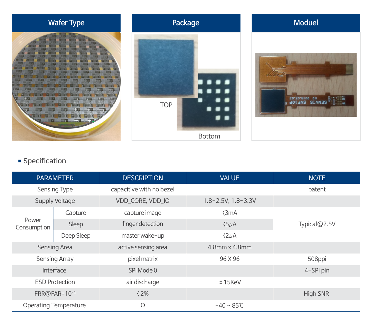
- Silicon based Capacitive type : Charge transfer integrator scheme based on Active Output
Voltage Feedback (AOVF). No bezel use
- Die size : 5,000μm x 6,000μm (array size : 96 x 96 : 4800μm x 4800μm)
- TSMC 0.25um CMOS Mixed 1P5M 2.5V & 3.3V including MIM
- Support 10MHz main operation with internal oscillator and up to 20MHz for Master interface
- Reliable image capture under the thickness of coated film up to 150μm
- Pipelined sensing for reducing image capture time
- Image capture time : 15ms @ 10MHz, memory read time : 7.5ms
- Ultra low power consumptions : normal operation : < 3mA @ 10MHz sleep mode : < 5μA, deep sleep mode : < 2μA
• Area type capacitive fingerprint ID sensor
•96 x 96 pixels (508 PPI)
•Die size : 5mm x 6mm
•AOVF scheme with ultra high sensitivity and low noise (patent)
•Operating frequency : 10MHz, Int. 180KHz
•Digital amplifier
•Embedded SRAM
•SPI interface with mode 0
•Supply voltage: 1.8~2.5V (Core), 1.8~3.3V(I/O)
•Best in class ESD : ± 15KV air discharge
•Operating temperature : -20 ~ 70 C°
•Foundry : TSMC 0.25um CMOS process
•Pipelined architecture for image capture
•Programmable gain amplifying with time integrations
• High SNR with the AOVF sensing
•No signal injection into finger
- No-bezel type
- Supports coating thickness up to 150um
• Area type capacitive fingerprint ID sensor
•Smartphones
•Tablets
•Wearable devices
•Smart Cards
•Safety Boxes
•Door Locks
•Security Devices

